
Journal of South China University of Technology(Natural Science) >
A Circuit Edit Method for ICs of Flip-Chip /Multilayer Interconnected Structure
Received date: 2020-03-17
Revised date: 2020-05-29
Online published: 2020-06-12
Supported by
Supported by the Key Realm R&D Program of Guangdong Province ( 2019B010145001)
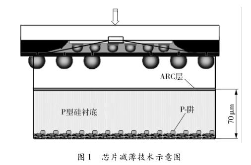
Flip-Chip packaging is an important packaging form for high-performance devices. Its unique packaging form brings new challenges to circuit-edit ( CE) . A CE method for ICs of flip-chip /multilayer interconnected structure was proposed in this paper by combining the techniques of thinning the back of the chip,deep and wide trench etching technology based on Focused Ion Beam ( FIB) ,trench etching endpoint monitoring based on dynamic grating diffraction fringes,and FIB circuit modification. Firstly,this method uses a global polishing thinning method to reduce the thickness of the flip-chip to about 70 μm. Then uses deep and wide trench etching technique and dynamic grating diffraction fringe-based trench etching endpoint monitoring technique to perform deep and wide Si trench etching. The chip is further thinned to about 4 μm,and then the circuit is edited with a FIB CE technique. The successful CE results of the M1 metal open circuit in a 6-layer metal CMOS chip show that the proposed method can effectively accomplish the modification of open or short circuit in flip-chip /multilayer interconnected structured ICs.
LIN Xiaoling, ZHANG Xiaowen, GAO Rui . A Circuit Edit Method for ICs of Flip-Chip /Multilayer Interconnected Structure[J]. Journal of South China University of Technology(Natural Science), 2020 , 48(12) : 63 -71 . DOI: 10.12141/j.issn.1000-565X.200118
/
| 〈 |
|
〉 |