Design of Two-point Modulation Phaselocked Loop for Polar Transmitter
 

Expand
  •  1. School of Electronic and Information Engineering,South China University of Technology,Guangzhou 510640,Guangdong,China; 2. Rising Micro Electronics Co. ,Ltd. ,Guangzhou 510006,Guangdong,China
梁振( 1979-) ,男,博士生,工程师,主要从事射频及混合信号集成电路研究

Received date: 2018-05-09

  Revised date: 2018-09-10

  Online published: 2019-01-02

Supported by

 Supported by the National Natural Science Foundation of China( 61604044, 61571196) 

Abstract

Two-point modulation phaselocked loop ( PLL) for Bluetooth polar transmitter was studied and designed by using 0. 11μm 1P6M CMOS process. In order to correct the loop gain of two phase modulation paths in the PLL and reduce the frequency shift keying error of using the phaselocked loop,a new gain correction method was proposed. And a new phaselocked loop circuit of two-point modulation based on gain calibration was proposed to reduce phase noise of PLL and accelerate the locking time of phaselocked loop. Chip measured results show that when voltage controlled oscillator oscillates at 4. 8 GHz,the phase noises at 10 kHz,1 MHz,3 MHz offsets are -83dBc/Hz, -108dBc/Hz and -114dBc/Hz,respectively. When using the polar transmitter of phaselocked loop to transmit the 0dBm signal,the FSK error is 2. 97%,and the phaselocked loop occupies 0. 32 mm2. The overall performance meets the requirements of Bluetooth RF chip test specification. 

Cite this article

LIANG Zhen LI Bin HUANG Mo XU Ken YE Hui 
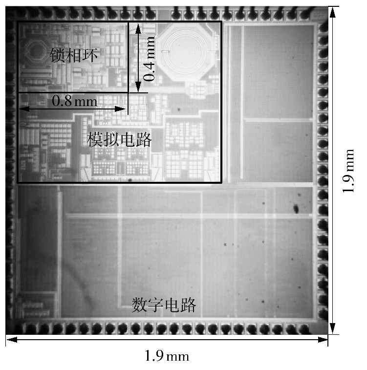
.

Design of Two-point Modulation Phaselocked Loop for Polar Transmitter
 
[J]. Journal of South China University of Technology(Natural Science), 2019 , 47(2) : 9 -15 . DOI: 10.12141/j.issn.1000-565X.180218

References

 
Outlines

/