华南理工大学学报(自然科学版) ›› 2022, Vol. 50 ›› Issue (12): 124-131.doi: 10.12141/j.issn.1000-565X.220143

所属专题: 2022年电子、通信与自动控制

• 电子、通信与自动控制 • 上一篇    下一篇

基于SiGe工艺的207~215 GHz工作带宽的紧凑型双向放大器

孟凡易 刘芷蘅 王毓 刘浩 马凯学   

  1. 天津大学 微电子学院,天津 300072
  • 收稿日期:2022-03-21 出版日期:2022-12-25 发布日期:2022-05-30
  • 通信作者: 孟凡易(1987-),男,博士,教授,主要从事毫米波、太赫兹集成电路设计研究。 E-mail:mengfanyi@tju.edu.cn
  • 作者简介:孟凡易(1987-),男,博士,教授,主要从事毫米波、太赫兹集成电路设计研究。
  • 基金资助:
    国家重点研发计划项目(2019YFB1803200)

A Compact Bidirectional Amplifier with 207~215 GHz Operating Bandwidth Based on SiGe Process

MENG Fanyi LIU Zhiheng WANG Yu LIU Hao MA Kaixue    

  1. School of Microelectronic,Tianjin University,Tianjin 300072,China
  • Received:2022-03-21 Online:2022-12-25 Published:2022-05-30
  • Contact: 孟凡易(1987-),男,博士,教授,主要从事毫米波、太赫兹集成电路设计研究。 E-mail:mengfanyi@tju.edu.cn
  • About author:孟凡易(1987-),男,博士,教授,主要从事毫米波、太赫兹集成电路设计研究。
  • Supported by:
    the National Key R&D Project of China(2019YFB1803200)

摘要:

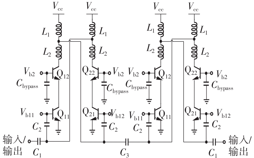
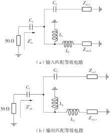
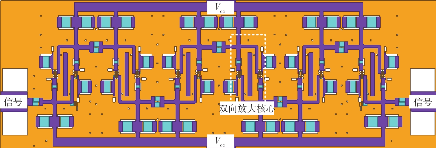
对称型双向放大器的接收、发射模式采用相同的放大核心,能够降低匹配网络结构的复杂度,减小芯片面积。为进一步降低对称型双向放大器芯片的面积,文中提出了一种融合不同工作状态下晶体管寄生参数的双向匹配技术,探明了在不同偏置状态下硅基晶体管的节点阻抗变化与匹配电路阻抗的映射关系;基于德国IHP微电子研究所0.13 μm SiGe BiCMOS工艺,采用该匹配技术,设计了一款207~215 GHz高增益、无开关式对称型双向放大器,该放大器通过对电路偏置的切换来实现消除通信系统中单刀双掷开关的目的。文中通过对芯片版图的镜像对称性进行优化来保证该双向放大器正向和反向性能的一致。全波电磁仿真和电路仿真结果表明:在工作频段内该双向放大器每个通道的最大增益为28.6 dB,最小噪声系数为16 dB,双向匹配网络的输入、输出反射系数S11S22的最小值分别为-13.6 dB、-15.5 dB,芯片功耗为63 mW,核心面积仅为0.17 mm2,说明该双向匹配网络在节省芯片面积的同时,能够实现优良的输入输出和噪声匹配效果;文中设计的无开关式硅基双向放大器可实现200 GHz以上的工作频率,具有高增益和面积紧凑的特点。该双向放大器极大地缩小了芯片面积,降低了射频前端成本,可应用于太赫兹微系统。

关键词: 硅基电路, 双向放大器, 无开关, 双向匹配网络, 微系统, 镜像对称性

Abstract:

The receiving and transmitting modes of symmetrical bidirectional amplifiers adopt the same amplifier core, which can reduce the complexity of matching network structure and reduce the chip area. In order to further reduce the area of the symmetrical bidirectional amplifier chip, this paper proposed a bidirectional matching technology which integrates the parasitic parameters of transistors under different working states, and explored the relationship between the node impedance variation of silicon-based transistors and the impedance of matching circuits under different bias states. Based on the Leibniz Institute for High Performance Microelectronics (IHP) 0.13 μm SiGe BiCMOS process, a 207~215 GHz high-gain, non-switching symmetrical bidirectional amplifier was designed. By switching the circuit bias, the amplifier realizes the purpose of eliminating the single-pole double-throw switch in the communication system. In this paper, the mirror symmetry of the chip layout was optimized to ensure the consistency of the forward and reverse energy of the amplifier. Full-wave electromagnetic simulation and circuit simulation results show that, in the working frequency band, the maximum gain of each channel of the bidirectional amplifier is 28.6 dB; the minimum noise figure is 16 dB; the minimum values of input and output reflection coefficients S11 and S22 of the bidirectional matching network are -13.6 dB, -15.5 dB respectively; the power consumption of the chip is 63 mW, and the core area is only 0.17 mm2. It shows that the bidirectional matching network can achieve excellent input, output and noise matching effect while saving chip area. The switchless silicon bidirectional amplifier designed in this paper can achieve the operating frequency of more than 200 GHz, and has the characteristics of high gain and compact area. The bidirectional amplifier greatly reduces the chip area and the cost of RF front-end, and can be applied to terahertz microsystems.

Key words: silicon-based circuit, bidirectional amplifier, switchless, bidirectional matching network, microsystem, mirror symmetry

中图分类号: